To use the Montreal subway, you tap a paper ticket against the turnstile and it opens. But how does it work? And how can the ticket be so cheap that it's disposable? I opened up the tiny NFC chip inside to find out more... 1/15
The Montreal Métro uses this paper ticket for occasional use. The gold chip is completely fake, just printed ink. But there's a different chip hidden inside... 2/15
Underneath the paper coating, the subway ticket contains a thin plastic sheet with a foil antenna printed on it. In the lower right, the tiny black speck is the NFC chip that makes it work. 3/15
The chip is about the size of a grain of salt. I took this photo under a microscope showing the NFC chip next to some salt. The black squares in the corner are where the antenna was attached. 4/15
How does the card work without a battery? The reader sends a signal through its antenna to the card's antenna. This signal both transmits data and powers the card. The two antennas are so close that they are coupled magnetically rather than by radio. 5/15
The card doesn't transmit a signal back. Instead it changes its antenna load, causing the card to absorb more or less energy from the reader. The reader detects this "load modulation", allowing it to receive data from the card without the card using power to transmit data. 6/15
I dissolved the chip's metal and oxide layers to reveal the chip's underlying silicon, showing the layout of its transistors. 7/15
This block diagram from the datasheet shows the components of the card. The RF interface is the analog circuitry connected to the antenna. The card stores 48 bytes (the ticket info) in the EEPROM. The digital circuitry accepts commands to read and write the EEPROM. 8/15
Most of the chip is digital logic, implemented with standard-cell circuitry, but there's lots of analog circuitry to handle the antenna signal. The four bond pads are where the antenna is attached. 9/15
Many chips use standard-cell circuitry. A program converts the logic description into rows of standardized blocks (NAND gates, flip-flops, etc.) and lays out the metal wiring between them. Much faster than creating an optimized layout by hand. 10/15
The photos are a bit blurry because the chip's smallest features are about 180 nm, smaller than the wavelength of light. The box indicates 5 connected transistors; the black lines are the gates of the transistors. Today's chips are an order of magnitude smaller. 11/15
Here's a closeup of the EEPROM, which holds the chip's data, similar to a very small flash drive. (I accidentally scratched it.) The driver circuitry to access the EEPROM is to the right and below. 12/15
My first attempt at removing the protective passivation layer on top of the chip didn't work. It just thinned the layer slightly, creating these wild colors from thin-film interference. I call this die photo the "tie die". 13/15

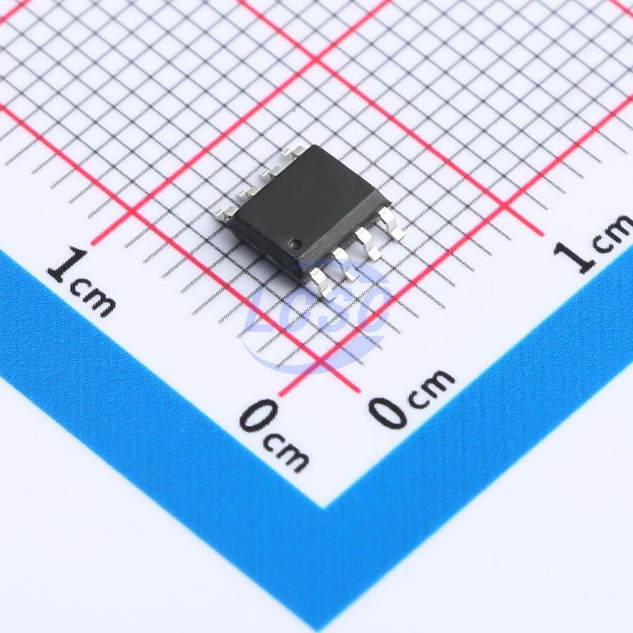
@kenshirriff is the EEPROM why it is so expensive? OTP Paduak chips are 2.5 cents in 10k quantities, which also includes the package: https://www.lcsc.com/product-detail/Microcontroller-Units-MCUs-MPUs-SOCs_PADAUK-Tech-PMS150C-S08_C129127.html